Add technical borders around the PCB.
If the PCB is small in size:
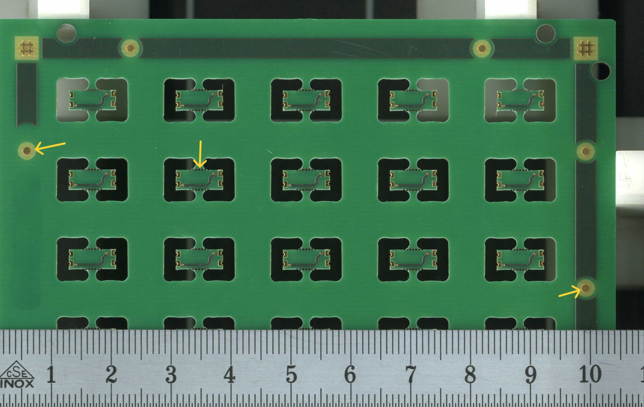
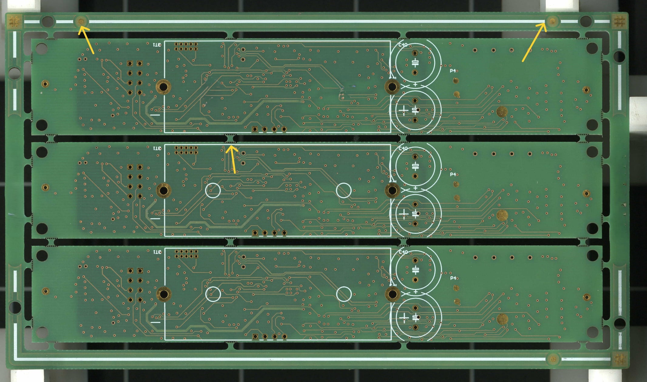
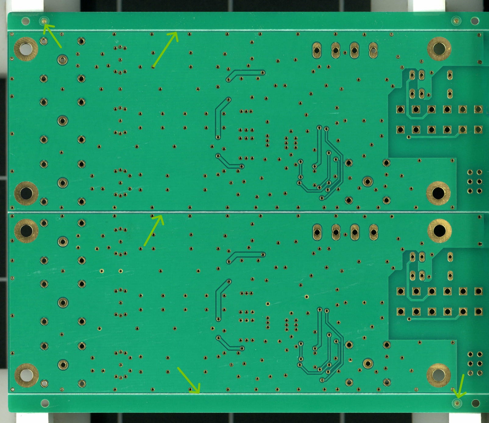
create a panel with technical borders and a separation between the boards.
Note: Always consult us before ordering your PCBs regarding the panel size/number of boards per panel.
The separation between the boards in the panel and the technical border can be either:
- Milled with perforated tabs (Perforated separators) or "routed"


- V-Cut / Scored

Insert fiducials on the short sides of the technical border (see yellow arrows in the examples of Perforated separators or V-Cut).
Always add at least
2 fiducials on your PCBs, on each side to be assembled in SMD – placed diagonally and at least 5mm from the edges of the board.
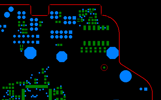
Examples of fiducials:
:

The ideal format for the fiducial:

Diameter: 1mm and free circular space around of +/- 1mm - No traces / silkscreen / Solder Resist – see image above and below:

Always add at least 2 fiducials on your PCBs, on each side to be assembled in SMD – placed diagonally and at least 5mm from the edges of the board.

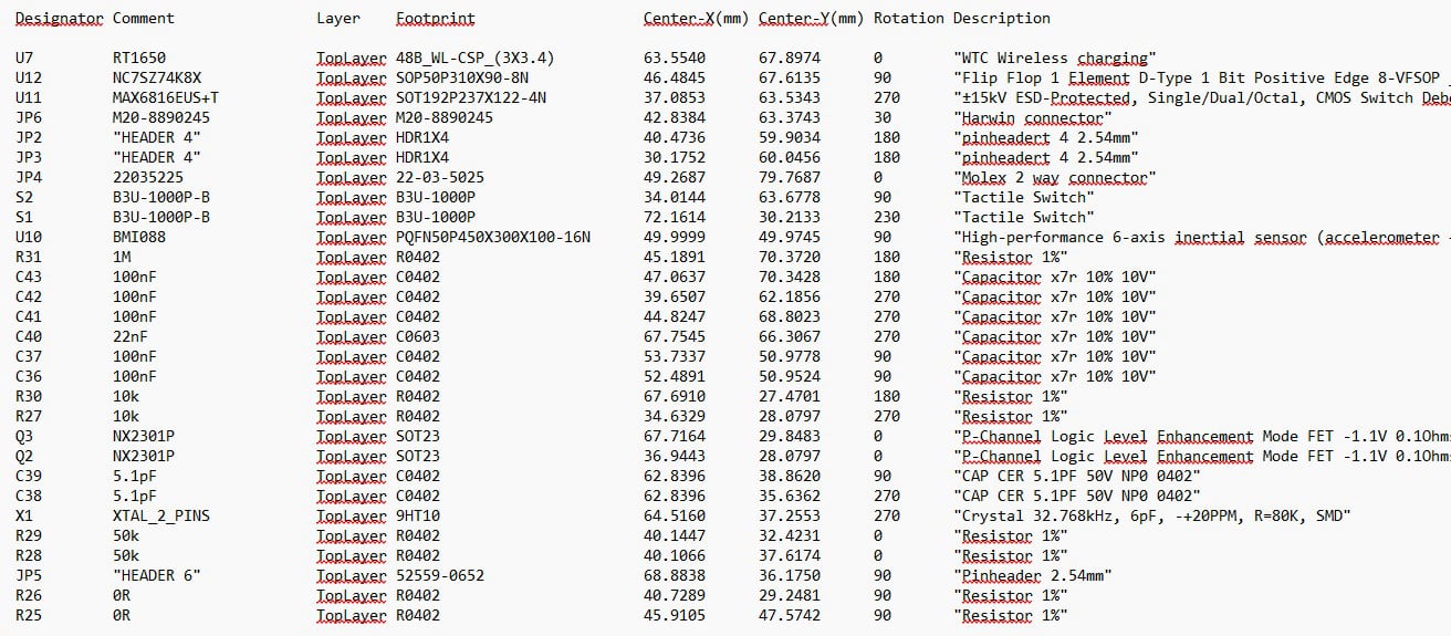
Define your fiducials as a component in your CAD library and include their coordinates in your Pick&Place file.

